Intel's Atom Architecture: The Journey Begins
by Anand Lal Shimpi on April 2, 2008 12:05 AM EST- Posted in
- CPUs
Building by FUBs
Below we have a conventional block diagram of the Intel Atom processor:

You'll see nine distinct blocks and in conventional microprocessor design at Intel, this is how the chip would be divided and conquered. You'd have one team working on the L2 cache, one team working on the IO interfaces, etc... Unfortunately the team at Austin was significantly smaller than your conventional microprocessor design group, so things had to be done a little differently.
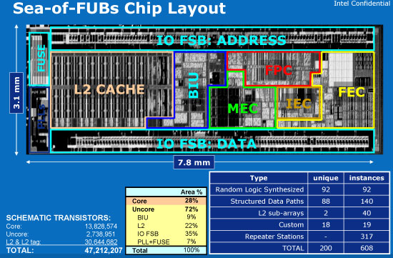
Intel calls the Atom approach a Sea-of-FUBs chip layout, a more granular approach to chip layout and design. A FUB (Functional Unit Block) is a floor-plannable object, an individual adder is a FUB, a decoder is a FUB, a cache is a FUB, etc... Because the size of each FUB made them more manageable, a single designer could handle multiple FUBs. The FUBs were also treated more modularly so that once a FUB was defined, designers can work on the FUB, chip integraters can give it to the layout guys and the timing guys can work in parallel as well. It allows for much more concurrent design than the conventional, more serial approach to chip design.
Approximately 90% of the fubs are built using standard Intel logic cells, minimizing the amount of custom work that needs to be done and decreasing the time to market on a processor like Atom. Minimizing the amount of custom Intel logic also means that it's easier to produce variants of Atom that may incorporate other important features depending on the target market.
The Sea-of-FUBs approach was also driven by a desire to keep power consumption and feature creep to a minimum. Area budgets were developed for each FUB and cluster of FUBs and Intel forced the designers to stick to these budgets. If a designer needed more die space for their FUB they couldn't just take it. A review board was setup where designers would come in and ask to grow their FUB. They were allowed to grow the FUB only if they were able to find another FUB that would shrink to accommodate it. The same thing applied for power.


46 Comments
View All Comments
lopri - Thursday, April 3, 2008 - link
This article is as much propagana-ish as it is technical. Did you read the last page of the article?clnee55 - Friday, April 4, 2008 - link
Since Anand wrote this article. I let him answer your accusationGulWestfale - Wednesday, April 2, 2008 - link
i believe that the graphics core in the chipset is a powerVR gen5 derivative; intel already uses some of their tech in its existing mainboards and wikipedia states that intel has licensed gen5 tech for one of its chipsets, the GMA500 (which is the same as poulsbo?) gen5 is also DX10-capable, which matches the info in your article.http://en.wikipedia.org/wiki/PowerVR#Series_5_.28S...">http://en.wikipedia.org/wiki/PowerVR#Series_5_.28S...
yyrkoon - Wednesday, April 2, 2008 - link
and wikipedia has been known to be wrong . . . a lot lately it seems.My point here *is*, I would probably trust anandtech more than wikipedia now days, as it seems any Joe can put up a 'reference' without citation.
jones377 - Wednesday, April 2, 2008 - link
Following the references link from the Wiki article...http://www.imgtec.com/News/Release/index.asp?NewsI...">http://www.imgtec.com/News/Release/index.asp?NewsI...
Poulsbo uses a PowerVR 3D core
Anand Lal Shimpi - Wednesday, April 2, 2008 - link
Yep, you guys are correct, I wasn't aware that it was public yet :) I've updated the article.Take care,
Anand